
Handle High-Frequency Prototype PCB Assembly
PCBs form the backbone of our modern electronic devices from smartphones to satellites. They carry signals, transmit power and manage heat to make the devices function. But what happens when these circuit boards operate at high frequencies?
High-frequency PCBs handle signals in the radio frequency (RF) and microwave ranges, ranging from hundreds of megahertz (MHz) to several gigahertz (GHz). They require specialized design and layout practices to ensure signal integrity and reliability. Poor design can lead to crosstalk, interference and other issues that can impact performance.
While low-frequency PCBs use traces to connect components, high-frequency PCBs require specific layout techniques to minimize noise and interference. This is because stray capacitance, inductance and transmission line effects that are negligible in low-frequency designs can significantly affect high-frequency signals.
To avoid these issues, you must consider signal path length and a number of other factors during high-frequency design. These include signal-to-noise ratio, EMI mitigation, and thermal management. You must also choose appropriate layer stack-up and materials to reduce skin effect losses and improve signal propagation. The use of higher-density circuitry and a smaller core size can also help to reduce the impact of signal loss.
Another important consideration is the choice of copper-clad laminate (CCL) material. A CCL with similar electrical properties to the component leads can prevent impedance discontinuities, ringing and ground bounce. It should also be compatible with the thermal expansion of the component to minimize stress and enhance long-term reliability.
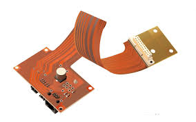
How to Handle High-Frequency Prototype PCB Assembly
Layer stack-up is also crucial for high-frequency designs. Ideally, a multilayer PCB should have a ground plane and a power plane positioned close to the signal layers. This allows the signals to be shielded and the current to return to its source, reducing interference. A good CCL and copper surface finish can also help to lower conductor loss and improve thermal management.
Lastly, a high-frequency PCB should be tested prior to being incorporated into end products. Testing approaches regarding thermal stress and solderability must be tailored to regulations such as IPC TM 650 2.6.8: 2004 and IPC J STD 003B: 2007A1. These tests will ensure that the circuit board can play its intended role in end products with minimal stress and maximum durability.
High-frequency prototype printed circuit board assembly is a challenging task because of its complex layers and the high number of vias. To ensure quality and consistency, you should use a professional PCB manufacturer with extensive experience in producing this type of product. A professional PCB manufacturer will employ a thorough inspection process to detect any defects or flaws during the production process and rectify them as needed. They will also be able to produce a high-frequency prototype PCB that meets all the required standards and specifications. In addition, the professional PCB manufacturer will provide fast turnaround times and competitive prices for your prototype. They will also provide a free quote for your project. This will allow you to compare quotes from different companies and find the best deal for your needs.


