
Signal Integrity Maintained on an RF Board
A PCB that is fabricated for use with radio frequencies, such as an RF board, requires specific materials and intricate processes in order to meet the stringent demands of high-frequency operation. This article delves into the nuances of this complex technology, uncovering important design considerations and best practices for maintaining signal integrity on RF boards.
RF boards are used to transmit and receive signals within a specified frequency range, making them essential for modern communication and mobile devices. In addition to a range of other critical features, these boards must be durable enough to withstand a variety of environmental conditions and operating temperatures. They must also be able to conduct significant amounts of heat, as well as efficiently dissipate this energy. In order to achieve this, a specialized manufacturing process is required for RF PCBs that takes into account high-frequency operation, temperature stability, and impedance matching.
The etching and drilling process that creates the foundation of a rf board requires precision in order to preserve the integrity of high-frequency signals. Using chemicals, unwanted copper is removed from the surface of the board to leave behind only the necessary traces, which are then drilled through with holes called vias in order to connect the different layers.
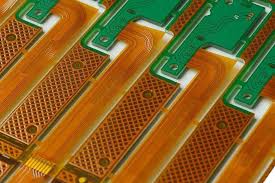
How Is Signal Integrity Maintained on an RF Board?
To maintain a consistent impedance throughout the circuit, manufacturers must design traces with precise width and spacing, taking into account the dielectric properties of the PCB material. They must also minimize the length of high-frequency signal paths to reduce the risk of loss and interference. In addition, manufacturers must test their RF boards with specialized equipment to evaluate their performance and identify any sources of distortion or impedance mismatches.
A variety of factors contribute to signal degradation and interference on an RF circuit, including electromagnetic noise (EMI), crosstalk, and thermal management. In order to minimize these problems, manufacturers must carefully design the layout of the traces and components, placing analog circuits near signal circuits and separating them from digital circuits to prevent crosstalk. They must also consider the placement of heat-generating components and ensure that they are adequately spaced from other traces in order to maximize efficiency and avoid temperature-related failures.
These systems rely on RF boards to process signals that detect obstacles, pedestrians, and other vehicles. In this context, the accuracy and speed of RF boards are crucial, as real-time processing of high-frequency data is needed for autonomous vehicles to make safe driving decisions. These boards must be designed to function in automotive environments, where factors like vibration, temperature extremes, and electromagnetic interference must be carefully considered. Additionally, the integration of RF boards with other sensor systems, such as cameras and infrared sensors, is key to achieving the level of reliability required for fully autonomous driving.
The reliability concerns that are unique to RF PCBs, such as solder joint failures and trace delamination, can be mitigated through careful design and material selection. In addition, specialized manufacturing techniques like controlled impedance testing and layer stack-up verification can help to reduce the likelihood of these defects. By implementing these strategies, manufacturers can ensure that their RF circuits perform at the highest levels of quality and functionality.

